XTPL Secures Second Japanese Customer for 3D Printed Electronics Packaging
Polish additive manufacturing company XTPL has announced its second sale in Japan, a new customer acquiring a Delta Printing System for validating copper conductive path printing for advanced semiconductor packaging.
XTPL, a manufacturer of printheads and 3D printers, has expanded its presence in the Japanese market with a new customer acquisition. This follows the company's initial entry into Japan just last month. The unnamed Japanese firm will utilize XTPL's Delta Printing System (DPS) to independently validate the company's technology for electronics packaging within its research and development laboratory.
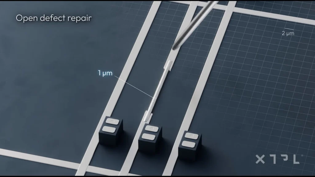
This latest sale includes a dedicated laser system, enabling the customer to print copper conductive paths. This capability is crucial for developing advanced packaging solutions for semiconductor technologies, including high-density interconnect (HDI) and ultra-high-density (UHD) printed circuit boards (PCBs) and semiconductor substrates. This aligns with XTPL's previous work in the Japanese market, indicating a growing demand for additive manufacturing in semicap equipment for packaging.
According to XTPL's CEO, Filip Granek, this new order represents a separate project from a previously announced sale of an Ultra Precise Dispensing (UPD) module. The customer has reached the third stage of XTPL's commercial model, progressing from joint validation tests to independent R&D validation. This demonstrates the replicability of XTPL's business strategy and its potential for repeat business with higher-value hardware.
XTPL's technology, utilizing copper nanoink, is being applied to yield management for HDI/UHD PCBs and semiconductor substrates used in advanced packaging. The company views Japan as a highly technologically advanced industrial market, making this second customer engagement significant for strengthening XTPL's global brand and commercial model.
XTPL's expansion into the Japanese market signifies a growing adoption of additive manufacturing for advanced semiconductor packaging. The ability to precisely print conductive paths with materials like copper nanoink is vital for creating complex System-in-a-Package (SiP) solutions, an alternative to traditional System-on-a-Chip (SoC) designs. This development aligns with the broader trend of miniaturization and increased functionality in electronics, potentially impacting sectors like consumer electronics and high-performance computing.
Edited by the news editor with AI from the original report — please refer to the original source.