Post-2030 Nanotechnological Additive Manufacturing of Dipole Antenna Arrays
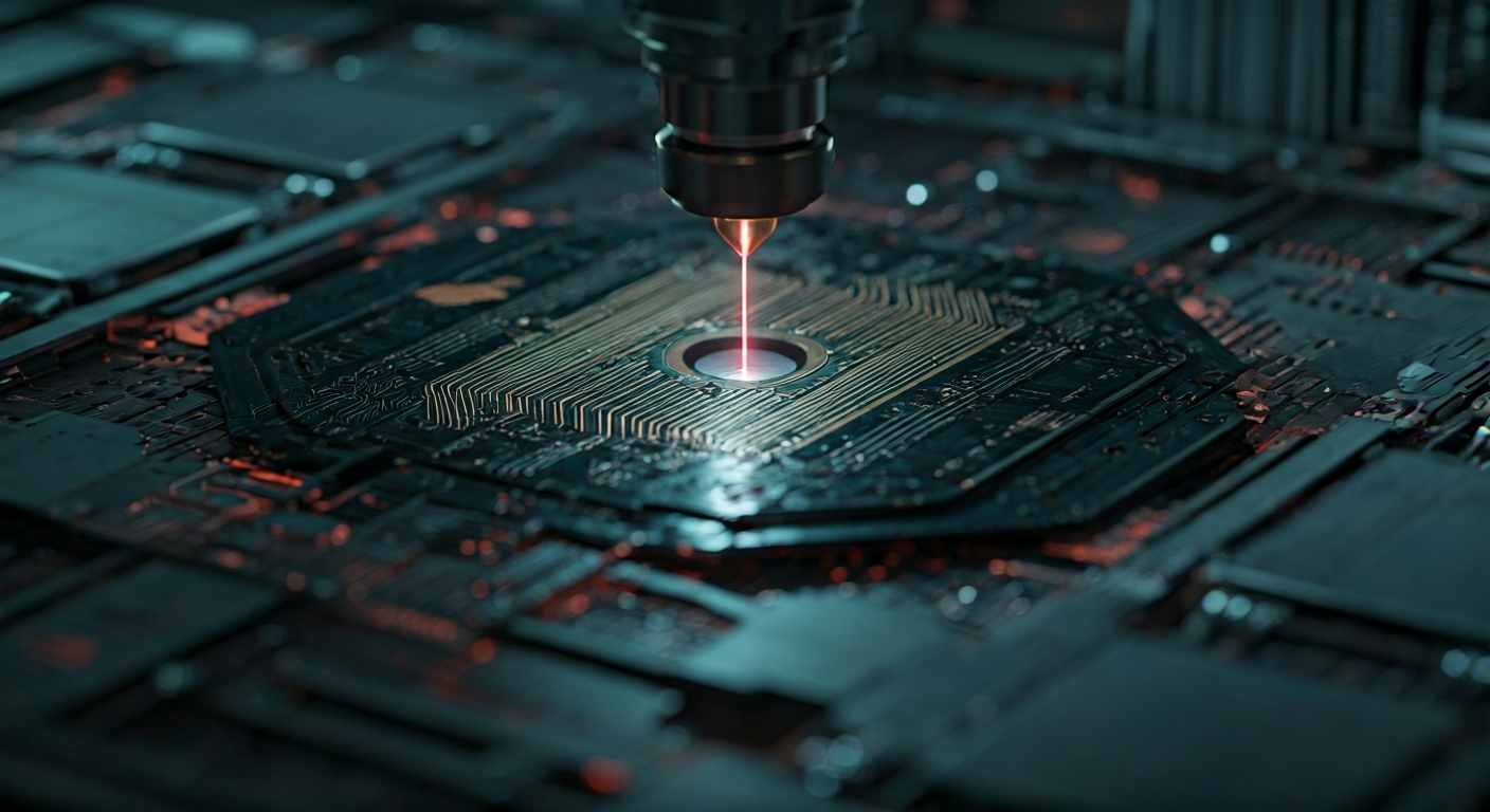
This document outlines a post-2030 manufacturing strategy for dipole antenna arrays using advanced nanotechnological additive manufacturing. The approach leverages novel nanomaterial feedstocks, sophisticated laser-based processes, precise piezoelectric actuation and nanopositioning, and AI-driven autonomous production lines to achieve high-performance, complex antenna structures with exceptional resolution and efficiency.
Target Device & Specifications
The target device is a reconfigurable dipole antenna array, designed for advanced communication systems, sensing, and potentially directed energy applications. Specifications include:
* **Frequency Range:** Tunable across K-band (18-27 GHz) to Ka-band (27-40 GHz), with potential for higher frequencies. * **Array Size:** Scalable from a few elements to hundreds or thousands, enabling beamforming and spatial multiplexing. * **Resolution:** Sub-wavelength feature control, allowing for precise shaping of individual dipoles and their spacing to optimize radiation patterns and impedance matching. * **Material Properties:** High electrical conductivity, low dielectric loss at operating frequencies, and excellent mechanical integrity. * **Reconfigurability:** Integrated active elements (e.g., varactors, MEMS switches) or intrinsic material properties enabling dynamic tuning of frequency, polarization, and beam direction. * **Environmental Robustness:** Capable of operating in harsh environments (e.g., vacuum, extreme temperatures, radiation).
Nanomaterial Feedstocks
The manufacturing process will rely on a diverse range of advanced nanomaterial feedstocks, specifically engineered for additive manufacturing:
* **Conductive Nanomaterials:** Plasmonically active metallic nanoparticles (e.g., gold, silver, copper) embedded in a photosensitive polymer matrix for high-resolution laser writing. Graphene nanoplatelets and carbon nanotubes (CNTs) will be used for their exceptional conductivity and mechanical strength, potentially as dopants or primary conductive elements. Metal-organic frameworks (MOFs) with high metal content will be explored for their ability to form dense metallic structures upon laser treatment. * **Dielectric Nanomaterials:** Low-loss dielectric nanoparticles (e.g., silica, alumina, specialized polymers) and engineered metamaterials with tailored refractive indices will be used for substrates, spacers, and dielectric loading to control electromagnetic properties. * **Active Nanomaterials:** Nanoscale piezoelectric materials (e.g., PZT nanoparticles, AlN nanowires) for integrated tuning mechanisms. Quantum dots or 2D materials (e.g., MoS2, WSe2) could be incorporated for tunable optical or electronic properties influencing antenna performance. * **Binder & Solvent Systems:** Photoinitiator-loaded, low-viscosity resins and specialized solvents designed for precise droplet dispensing and rapid curing under laser irradiation.
Nanoscale Additive & Laser Process
The core fabrication will employ a synergistic combination of advanced laser-based additive manufacturing techniques:
* **Two-Photon / Multiphoton Lithography (TPL/MPL):** For creating intricate 3D structures with sub-100 nm resolution. This will be used for fabricating complex dielectric substrates, precise positioning of individual nanoscale antenna elements, and creating metamaterial structures that enhance antenna directivity and bandwidth. * **Femtosecond Laser Direct Writing (fs-DLW):** Utilizing focused femtosecond laser pulses to induce localized chemical or physical changes in the feedstock material. This will be employed for direct writing of conductive traces from nanoparticle-infused resins, creating highly conductive pathways with minimal scattering losses. It will also be used for selective curing and densification of printed structures. * **Laser-Induced Forward Transfer (LIFT):** For precise, non-contact deposition of individual nanoscale components or material droplets. This technique will be crucial for placing pre-fabricated functional nanostructures (e.g., active elements, specific metamaterial units) onto the printed antenna array or for depositing highly concentrated metallic nanoparticle inks to form dense conductive elements. * **Nanoscale Selective Laser Sintering (nSLS):** Adapted for nanoscale powders or nanoparticle inks. This process will enable the sintering of metallic nanoparticle feedstocks into continuous, highly conductive metallic structures, ideal for forming the dipole arms and feeding networks of the antenna array.
Piezoelectric & Nanopositioning Integration
Achieving the required precision for sub-wavelength antenna features and integrated functionalities necessitates advanced actuation and positioning systems:
* **Piezoelectric Actuators:** High-precision, multi-axis piezoelectric stages (e.g., flexure-based piezo stages) will provide the primary motion control for the laser optics and/or the build platform. These will enable sub-nanometer resolution movement, crucial for precise placement of individual antenna elements and for fine-tuning the laser focus. * **Nanopositioning Systems:** Integration of advanced nanopositioning systems, potentially including atomic force microscope (AFM) based manipulators or interferometric position sensors, will ensure sub-nanometer absolute and relative positioning accuracy during the additive process. This is critical for aligning multiple laser beams, controlling material deposition, and ensuring perfect alignment of antenna elements and integrated components. * **Integrated Actuation:** Piezoelectric materials will also be directly printed as part of the antenna structure itself, enabling in-situ reconfigurability of the antenna elements for dynamic beam steering or frequency tuning, controlled by external electric fields applied to the printed piezoelectric components.
Autonomous Production Line
The manufacturing will be orchestrated by an AI-driven autonomous production line:
* **AI Design & Optimization:** Machine learning algorithms will generate optimal antenna designs based on performance requirements, material properties, and fabrication constraints. They will also predict and compensate for process variations. * **Self-Directed Fabrication:** The AI will manage the entire fabrication process, dynamically adjusting laser parameters, material feed rates, positioning trajectories, and curing conditions in real-time based on sensor feedback. * **In-Situ Monitoring & Feedback:** Integrated optical microscopy, spectroscopy, and potentially electrical probing will provide real-time feedback on material deposition, feature formation, and early-stage electrical performance. AI will analyze this data to identify defects and initiate corrective actions. * **Self-Assembly & Calibration:** Advanced AI will coordinate the assembly of complex multi-component antenna arrays, potentially guiding self-assembling nanomaterials or precisely placing pre-fabricated functional units. Automated calibration routines will ensure the final device meets specifications. * **Robotic Handling & Logistics:** Automated robotic systems will manage feedstock replenishment, waste removal, and the transfer of printed components to subsequent processing or testing stages.
Key Challenges & Yield
Key challenges include:
* **Material Homogeneity & Stability:** Ensuring consistent properties of nanomaterial feedstocks and their long-term stability under processing conditions. * **Defect Control:** Minimizing voids, inconsistencies, and contamination during nanoscale printing, which can significantly degrade antenna performance. * **Interconnects & Transitions:** Achieving low-loss electrical connections between different printed materials and to external circuitry. * **Scalability & Throughput:** Transitioning from high-resolution, low-volume laboratory demonstrations to high-throughput industrial manufacturing. * **Metamaterial Integration:** Precisely fabricating complex metamaterial structures that exhibit desired electromagnetic properties.
Yield will initially be low, requiring robust in-situ metrology and AI-driven process control to identify and mitigate defects. Iterative design and process refinement will be crucial for improving yield over time.
Test & Qualification
Rigorous testing and qualification protocols will be implemented:
* **Electrical Performance:** S-parameter measurements (S11, S21), radiation pattern characterization, gain, efficiency, and impedance matching measurements in anechoic chambers. * **Material Characterization:** Electron microscopy (SEM, TEM) for structural integrity and feature resolution, atomic force microscopy (AFM) for surface topography, X-ray diffraction (XRD) for crystalline structure, and electrical conductivity measurements. * **Environmental Testing:** Exposure to simulated space/Martian conditions (vacuum, thermal cycling, radiation) to assess durability. * **Functional Testing:** Verification of reconfigurability and dynamic tuning capabilities.
TRL & Post-2030 Roadmap
This technology is envisioned to be at TRL 4-5 in the near-term (2025-2030), focusing on component-level demonstrations. The post-2030 roadmap targets:
* **2030-2035:** Integrated demonstration of a functional reconfigurable dipole antenna array with basic AI control and improved yield (TRL 6-7). * **2035-2040:** Autonomous production line for complex antenna arrays with advanced metamaterial integration and high throughput (TRL 8). * **2040+:** Widespread adoption in advanced communication, sensing, and space applications, with potential for in-situ manufacturing capabilities (TRL 9).
Applications (incl. in-situ fabrication in space/Mars)
Applications are broad and include:
* **Advanced Wireless Communication:** High-gain, reconfigurable antennas for 6G/7G networks, satellite communication, and IoT. * **Sensing & Radar:** Miniaturized, high-performance antennas for ground-penetrating radar, medical imaging, and environmental monitoring. * **Space & Planetary Exploration:** Lightweight, robust, and reconfigurable antennas for deep space probes, orbital platforms, and surface rovers. **Crucially, the autonomous nature of this manufacturing process makes it ideal for in-situ fabrication on the Moon or Mars.** Using local regolith (processed into usable nanomaterials) and minimal Earth-based resupply, antenna arrays can be fabricated on demand for communication, scientific instruments, and power transmission, significantly enhancing mission self-sufficiency and reducing launch costs. * **Defense & Security:** Adaptive and stealthy antenna systems. * **Metamaterial Devices:** Antennas with novel electromagnetic properties for cloaking, energy harvesting, and advanced sensing.
Cross-Model Verification (GPT-3.5)
- The proposed specifications and applications for the reconfigurable dipole antenna array are scientifically sound and feasible for post-2030 developments in advanced communication and sensing systems. - The use of advanced nanomaterial feedstocks, including conductive, dielectric, and active nanomaterials, for additive manufacturing of the antenna array aligns with current trends in materials science and nanotechnology. - The nanoscale additive manufacturing processes described, such as Two-Photon Lithography and Laser-Induced Forward Transfer, are plausible for achieving high-resolution and complex structures in antenna fabrication. - The integration of piezoelectric actuators and nanopositioning systems for precision placement of antenna elements and in-situ reconfigurability is within the realm of advanced manufacturing technologies. - The concept of an AI-driven autonomous production line for managing the fabrication process, optimizing designs, and providing real-time feedback aligns with the industry's trajectory towards smart manufacturing systems.
On-demand nanomanufacturing of components like dipole antenna arrays is a cornerstone for a self-sufficient multi-planetary civilization. It enables the creation of essential infrastructure (communication, sensing, power) using local resources and minimal Earth dependency. This capability drastically reduces launch mass, cost, and lead times, fostering rapid expansion and resilience. By fabricating complex, high-performance devices *in situ*, humanity can establish truly independent outposts, capable of self-repair and adaptation in alien environments.
This content was produced by the news editor with AI.