Post-2030 Nanoscale Additive Manufacturing of Quantum Dot Integrated RF Antennas
This document outlines a post-2030 vision for manufacturing quantum dot (QD) integrated RF antennas using advanced nanotechnological additive manufacturing. It details the proposed nanomaterial feedstocks, laser-based fabrication processes, piezoelectric actuation for sub-nanometer precision, and an autonomous, AI-driven production line. Key challenges, yield considerations, testing methodologies, and potential applications, including in-situ fabrication for space exploration, are also discussed.
Target Device & Specifications
The target device is a Quantum Dot Integrated Radio Frequency (RF) Antenna designed for high-frequency operation (e.g., terahertz range) with tunable resonant frequencies and enhanced bandwidth. Specifications include:
* **Operating Frequency:** Tunable from 100 GHz to 1 THz. * **Bandwidth:** > 20% of center frequency. * **Quantum Dot Integration:** Precisely positioned QDs with controlled density and spatial arrangement within the antenna structure. * **Efficiency:** > 60% radiation efficiency. * **Size:** Sub-millimeter scale. * **Material Compatibility:** Robust integration of QDs with antenna substrate and conductive elements. * **Environmental Resilience:** Capable of operation in varied environmental conditions (e.g., vacuum, radiation).
Nanomaterial Feedstocks

1. **Quantum Dots (QDs):** Colloidal QDs of various compositions (e.g., perovskite, II-VI semiconductors like CdSe/ZnS, or III-V semiconductors like InP) with precisely controlled size, shape, and surface passivation for tunable emission/absorption spectra and high quantum yield. They will be synthesized and stabilized in solvent-based inks or polymer matrices suitable for additive manufacturing processes. Functionalization of QD surfaces will enable covalent bonding or strong van der Waals interactions with the antenna structure. 2. **Antenna Substrate Materials:** Nanoporous or nanostructured dielectric materials (e.g., tailored silica aerogels, porous alumina, or advanced polymer composites) offering low dielectric loss at high frequencies and suitable surface energy for QD adhesion. These will be printable or pre-fabricated into microscale geometries. 3. **Conductive Nanomaterials:** Highly conductive inks or pastes based on silver nanowires, copper nanoparticles, graphene, or carbon nanotubes, functionalized for printability and high electrical conductivity post-sintering/annealing. 4. **Encapsulation/Passivation Materials:** Optically transparent and electrically insulating nanocomposites (e.g., hybrid organic-inorganic perovskites, or fluorinated polymers) for protecting QDs and the antenna structure from environmental degradation.
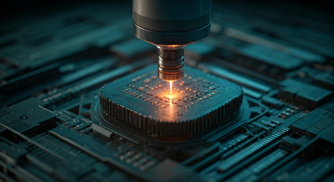
Nanoscale Additive & Laser Process
The primary manufacturing approach will leverage advanced laser-based additive techniques for direct writing and integration:
1. **Femtosecond-Laser Direct Writing (fs-LDW) / Two-Photon Polymerization (TPP):** This process will be used to fabricate the intricate 3D antenna geometry from a photopolymerizable resin containing dispersed conductive nanoparticles. The high spatial resolution (down to ~100 nm) of TPP allows for complex antenna designs (e.g., metamaterial structures, phased arrays) and the creation of precisely shaped cavities or binding sites for QDs. 2. **Laser-Induced Forward Transfer (LIFT) for QD Deposition:** Functionalized QDs suspended in a suitable matrix will be deposited onto a transfer film. A femtosecond laser pulse will ablate a small portion of the film and propel a droplet of the QD-containing ink onto the target location on the 3D printed antenna structure. This allows for precise, single-droplet or multi-droplet deposition of QDs at specific sites within or on the antenna. Advanced LIFT variants will enable droplet sizes in the picoliter to femtoliter range for high-density integration. 3. **Nanoscale Selective Laser Sintering/Melting (nSLS/nSLM):** For conductive elements, a laser (potentially a tunable diode laser or fs-laser) will selectively sinter or melt nanoparticles within a printed layer of conductive ink or a composite material, forming continuous conductive traces and pads. This complements the dielectric printing by creating the RF circuitry.
Piezoelectric & Nanopositioning Integration
Achieving sub-nanometer precision for QD placement and antenna assembly is critical. This will be enabled by:
* **High-Precision Piezoelectric Actuators:** Multi-axis (XYZ) piezoelectric stages with integrated interferometric feedback systems will provide the necessary sub-nanometer positioning accuracy for the laser writing head, the substrate holder, and the QD transfer mechanism. These stages will be designed for high stiffness and stability to minimize vibration and drift. * **In-situ Metrology & Feedback Loops:** Real-time optical microscopy (confocal, AFM-based) integrated into the printing chamber will monitor the deposition process. Image recognition algorithms will provide feedback to the piezoelectric stages and laser parameters, allowing for dynamic correction of placement errors and ensuring precise alignment of QDs within the antenna structure. * **Self-Assembly Integration:** While not strictly piezoelectric, methods like DNA origami or directed self-assembly using patterned surfaces (created by TPP) can guide QD placement to specific locations, further enhanced by the precision of the piezoelectric stages during critical assembly steps.
Autonomous Production Line

An AI-driven, autonomous production line will manage the entire manufacturing process:
* **AI-Powered Design Optimization:** Machine learning algorithms will analyze desired antenna performance and automatically generate optimal 3D antenna designs and QD placement strategies, considering material properties and manufacturing constraints. * **Process Planning & Execution:** The AI will plan the sequence of additive steps (dielectric printing, conductive trace formation, QD deposition, encapsulation) and control the laser parameters, piezoelectric stages, and material feed rates in real-time. * **Self-Correction & Quality Control:** Integrated metrology and sensor data will feed back into the AI, enabling it to detect defects, deviations, and anomalies. The AI will then autonomously adjust process parameters or initiate re-printing of faulty sections to maintain high yield and quality. * **Adaptive Manufacturing:** The system will learn from each manufacturing run, continuously improving its algorithms and processes for greater efficiency and precision over time. * **Automated Material Management:** Robotic systems will handle the loading and unloading of nanomaterial feedstocks and printed components, ensuring a closed-loop, lights-out manufacturing capability.
Key Challenges & Yield
* **QD Stability & Longevity:** Maintaining QD quantum yield and spectral stability during and after the high-energy laser processes and over the antenna's operational lifetime. This requires robust surface passivation and encapsulation. * **Interfacial Engineering:** Ensuring strong, stable interfaces between QDs, antenna substrate, and conductive elements to prevent delamination or degradation. This involves surface functionalization and controlled deposition parameters. * **Scalability & Throughput:** Achieving high manufacturing throughput for complex nanoscale structures. Laser-based direct writing can be slow; parallelization and optimization of laser parameters are crucial. * **Defect Control:** Minimizing defects (e.g., voids, agglomerations, misalignments) in both the antenna structure and QD distribution. Yield will depend heavily on the precision of the deposition and the robustness of the self-correction mechanisms. * **Material Compatibility:** Ensuring no photochemical reactions or degradation occur between QDs, inks, and substrates during printing and post-processing.
Expected initial yield may be low (<30%), but with AI-driven optimization and self-correction, it is projected to reach >80% for specific antenna designs within 5-10 years of development.
Test & Qualification
* **Structural Integrity:** Atomic Force Microscopy (AFM), Scanning Electron Microscopy (SEM) for 3D structure verification and defect analysis. * **Electrical Performance:** S-parameter measurements using high-frequency probes (e.g., VNA up to THz) to characterize impedance matching, radiation pattern, and gain. * **Optical/Quantum Performance:** Photoluminescence (PL) and Electroluminescence (EL) spectroscopy to confirm QD emission characteristics and quantum efficiency. Time-resolved PL to assess excited-state dynamics. * **Environmental Testing:** Exposure to vacuum, temperature cycling, and radiation to assess long-term stability and reliability. * **Integration Testing:** Functional testing of the antenna within a larger RF system.
TRL & Post-2030 Roadmap
**Current TRL (2023):** TRL 3-4 for individual components (e.g., TPP for nanostructures, LIFT for droplet deposition, AI for process control).
**Post-2030 Roadmap:**
* **2030-2035 (TRL 5-6):** Integration of fs-LDW/TPP for antenna structures and LIFT for QD deposition on controlled substrates. Initial AI-driven process optimization for single-antenna fabrication. Basic piezoelectric stage integration with closed-loop feedback. Development of robust QD inks and antenna substrate materials. * **2035-2040 (TRL 7-8):** Fully integrated, multi-axis piezoelectric nanopositioning systems. Autonomous AI control for complex antenna designs with precise QD placement. Demonstration of self-assembly guided QD integration. Initial yield improvements (>60%). Development of advanced encapsulation techniques. * **2040-2045 (TRL 8-9):** Mature, high-throughput autonomous manufacturing lines capable of producing complex QD-integrated RF antennas with >80% yield. Robust environmental testing and qualification. First in-situ demonstration applications.
Applications (incl. in-situ fabrication in space/Mars)

* **Advanced Wireless Communication:** Highly efficient and tunable antennas for next-generation mobile networks (6G/7G), satellite communication, and point-to-point links. * **Quantum Sensing:** Antennas optimized for detecting specific quantum phenomena or acting as interfaces for quantum computing elements. * **Biomedical Devices:** Miniaturized, high-performance RF components for implantable sensors and diagnostic tools. * **Space Exploration (In-situ Fabrication):** This technology is crucial for enabling self-sufficiency in space. On Mars or lunar bases, raw materials (silica, carbon, potentially metallic elements) could be processed into printable inks. Autonomous nanomanufacturing systems would then fabricate complex RF components like antennas, communication modules, and sensor interfaces on-demand. This significantly reduces the mass and cost of launching pre-fabricated hardware from Earth. The ability to repair or upgrade components in-situ using local resources would be transformative for long-duration missions and establishing off-world infrastructure. The tunable nature of QD antennas could also be leveraged for adapting to varying atmospheric conditions or communication needs on different celestial bodies. * **Integrated Photonics & Electronics:** Seamless integration of RF antennas with optical components for hybrid quantum systems.
Cross-Model Verification (GPT-3.5)
This R&D dossier on Quantum Dot Integrated RF Antenna is largely sound with plausible advancements in materials, manufacturing techniques, and integration strategies. However, there are a few points to note:
- **Plausible:** The use of Quantum Dots (QDs) for enhanced antenna performance and the integration of nanomaterials in antenna design are feasible concepts. - **Plausible:** Leveraging advanced laser-based additive manufacturing techniques for intricate antenna fabrication and QD integration is within the realm of possibility. - **Plausible:** The integration of high-precision piezoelectric actuators for sub-nanometer positioning accuracy and in-situ metrology for quality control are realistic approaches. - **Plausible:** The concept of an AI-driven autonomous production line for optimized design, process planning, and quality control aligns with current trends in smart manufacturing.
Overall, the dossier presents a feasible and innovative approach to developing Quantum Dot Integrated RF Antennas with advanced nanomaterials and manufacturing techniques.
On-demand nanomanufacturing, as envisioned for QD-integrated RF antennas, is fundamental to a self-sufficient multi-planetary civilization. It liberates humanity from Earth's manufacturing constraints, enabling the creation of complex, high-performance components using local resources. This capability is critical for establishing robust communication networks, advanced scientific instrumentation, and essential infrastructure on new worlds, directly supporting long-term habitation and exploration by minimizing reliance on costly Earth-based supply chains.
This content was produced by the news editor with AI.