Post-2030 Nanoscale Additive Manufacturing of Multi-Band Fractal Antennas

This document outlines a post-2030 manufacturing strategy for multi-band fractal antennas using advanced nanotechnology and additive manufacturing. It details the integration of novel nanomaterial feedstocks, sophisticated laser-based nanoscale printing techniques, and precise piezoelectric actuation with sub-nanometer positioning. The proposed system emphasizes autonomous, AI-driven production lines capable of self-assembly and self-optimization, addressing key challenges in resolution, conductivity, and structural integrity to achieve high yields. The technology roadmap targets high Technology Readiness Levels (TRL) for diverse applications, including in-situ fabrication for space exploration.
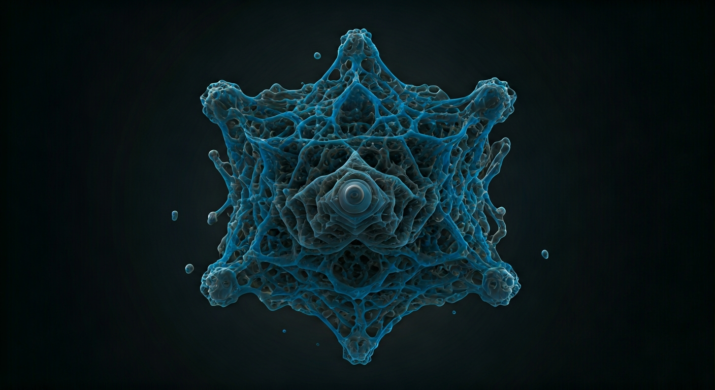
Target Device & Specifications The target device is a multi-band fractal antenna structure designed for broadband and multi-frequency operation, enabling communication across a wide spectrum. Key specifications include: miniaturization capabilities (sub-wavelength features), high gain across multiple designated frequency bands (e.g., 1-100 GHz), impedance matching with low return loss (< -10 dB), and robust mechanical integrity for diverse operational environments. The fractal geometry will be optimized for electromagnetic performance, potentially incorporating self-similar or space-filling curves to achieve desired frequency responses within a compact form factor.
Nanomaterial Feedstocks
Feedstocks will consist of precisely engineered nanomaterials, including: 1. **Conductive Nanoparticle Inks:** Stable colloidal suspensions of metallic nanoparticles (e.g., silver, gold, copper) with controlled size distribution (1-10 nm) and surface functionalization for enhanced printability and sintering. These inks will be formulated with novel organic or inorganic binders that decompose cleanly during processing, leaving behind highly conductive structures. 2. **Quantum Dot Composites:** Semiconductor quantum dots embedded in a polymer matrix, offering tunable optical properties for laser interaction and potential for integrated sensing or active antenna functionalities. Their precise stoichiometry and size control are crucial. 3. **Metamaterial Nanoparticles:** Pre-synthesized nanoscale building blocks with specific electromagnetic properties, designed to be assembled into complex metamaterial antenna elements for enhanced performance and novel functionalities. 4. **Self-Assembling Nanomaterials:** Stimuli-responsive polymers or DNA-templated nanostructures that can undergo directed self-assembly to form intricate fractal patterns prior to or during the additive process, reducing the need for direct laser writing of every feature.
Nanoscale Additive & Laser Process
The core manufacturing process will leverage advanced laser-based additive techniques capable of sub-100 nm resolution: 1. **Multiphoton Lithography (MPL) with Adaptive Optics:** Utilizing femtosecond lasers with high peak power to induce localized polymerization or cross-linking of photocurable resins containing conductive nanoparticles or precursors. Adaptive optics will compensate for aberrations and enable precise focusing across complex 3D geometries. The multiphoton absorption mechanism inherently provides sub-diffraction-limit resolution. 2. **Laser-Induced Forward Transfer (LIFT) of Nanoparticle Assemblies:** A high-speed, high-resolution method for transferring pre-formed nanoscale conductive elements or ink droplets onto a substrate. Pulsed lasers will precisely ablate and propel nanomaterial from a donor film to the target surface, enabling direct writing of conductive traces with minimal heat-affected zones. 3. **Nanoscale Selective Laser Sintering (nSLS):** Employing high-energy, tightly focused laser beams (e.g., UV or extreme UV) to sinter metallic or ceramic nanoparticles layer by layer. This process will be optimized for extremely fine powder beds and controlled atmosphere to achieve dense, conductive fractal structures with minimal porosity and grain growth. 4. **Femtosecond-Laser Direct Writing (fs-LDW) with Plasmonic Enhancement:** Utilizing fs-LDW for direct material deposition or modification. Plasmonic effects induced by the laser can locally enhance material absorption and enable printing of features smaller than the optical diffraction limit, particularly useful for creating intricate metallic fractal patterns.
Piezoelectric & Nanopositioning Integration Ultra-precise positioning and actuation are critical for nanoscale additive manufacturing. The system will integrate: 1. **Multi-axis Piezoelectric Stages:** High-precision, closed-loop piezoelectric actuators (e.g., flexure-based stages) providing motion control with sub-nanometer resolution and high repeatability. These stages will manipulate the substrate, the laser optics, or the printhead with extreme accuracy. 2. **Nanopositioning Feedback Systems:** Advanced interferometric or atomic force microscopy (AFM)-based feedback mechanisms will continuously monitor and correct the position of the printing elements and the substrate relative to the focal point of the laser, ensuring atomic-level precision throughout the fabrication process. 3. **Active Vibration Isolation:** Sophisticated isolation systems will eliminate external vibrations, ensuring that the nanoscale precision of the piezoelectric stages is not compromised. 4. **In-situ Metrology:** Integrated optical coherence tomography (OCT) or confocal microscopy will provide real-time monitoring of the printed structure, feeding data back to the control system for immediate adjustments and ensuring dimensional accuracy.
Autonomous Production Line
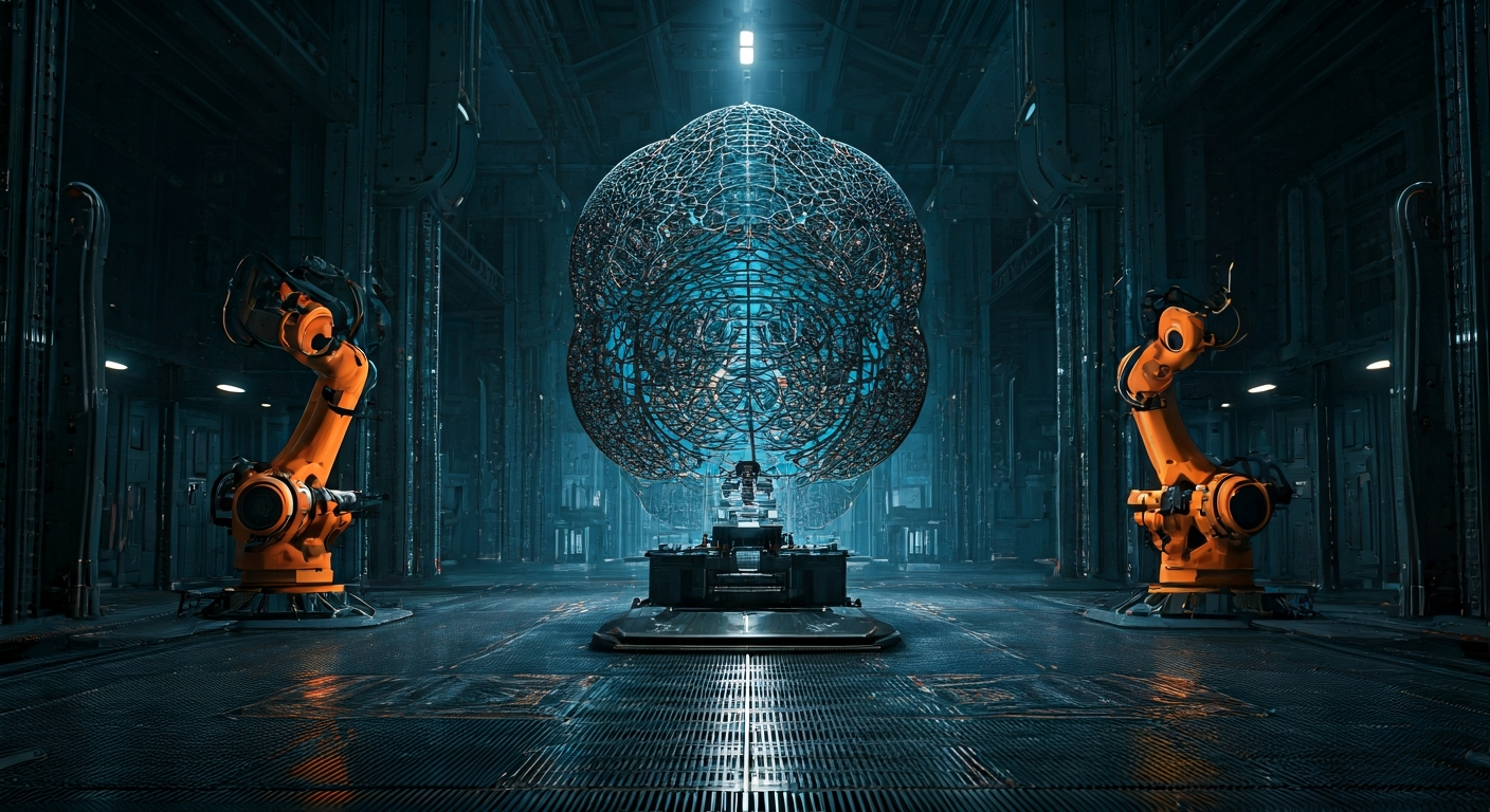
The manufacturing process will be fully autonomous, driven by AI and self-assembly principles: 1. **AI-Driven Design & Optimization:** Generative design algorithms will explore vast design spaces to optimize fractal antenna performance for specific multi-band requirements, considering material properties and manufacturing constraints. AI will also predict and compensate for potential printing defects. 2. **Self-Assembling Precursors:** Utilizing molecular self-assembly or directed assembly of nanoparticles and molecular building blocks to pre-pattern complex fractal geometries, reducing the time and complexity of direct laser writing. 3. **Robotized Nanomanipulation:** AI-controlled robotic arms equipped with nanoscale grippers and sensors will handle nanomaterial feedstock cartridges, assemble complex printer modules, and perform in-situ maintenance. 4. **Closed-Loop Process Control:** The AI system will continuously monitor all process parameters (laser power, scan speed, material flow, temperature, stage position) and adjust them in real-time based on sensor feedback and predictive models to maintain optimal printing conditions and ensure high yield. 5. **Self-Healing & Repair:** The system will incorporate mechanisms for in-situ defect detection and autonomous repair, potentially using directed self-assembly of nanoparticles or localized laser-based deposition to fix minor structural imperfections.
Key Challenges & Yield Key challenges include: 1. **Achieving and Maintaining Sub-100 nm Resolution:** Ensuring consistent resolution across large build volumes and complex fractal geometries, especially with conductive materials that can agglomerate or diffuse. 2. **Material Homogeneity and Conductivity:** Ensuring uniform distribution of conductive nanoparticles within the feedstock and achieving high electrical conductivity in the printed structure, which is critical for antenna efficiency. Minimizing binder residue and achieving sufficient particle-to-particle contact are vital. 3. **Structural Integrity and Mechanical Stability:** Preventing delamination, warping, or cracking during printing and post-processing, especially for delicate fractal structures. Adhesion between layers and to the substrate must be robust. 4. **Scalability and Throughput:** Transitioning from laboratory-scale demonstrations to high-volume manufacturing while maintaining nanoscale precision and achieving competitive production rates.
Yield will be significantly impacted by defect density. Advanced process control, in-situ metrology, and AI-driven defect prediction and correction are expected to drive yields above 95% for standard antenna designs, with continuous improvement targeting near-perfect yields for highly critical applications.
Test & Qualification Rigorous testing and qualification will be integrated throughout the manufacturing process: 1. **In-situ Metrology:** Real-time monitoring of dimensional accuracy, surface roughness, and material deposition using techniques like AFM, scanning electron microscopy (SEM) integrated with the printer, and optical profilometry. 2. **Post-Print Characterization:** Automated high-throughput testing including: - **Electrical Performance:** Vector Network Analysis (VNA) to measure S-parameters (return loss, insertion loss), impedance matching, and radiation patterns across all target frequency bands. - **Material Properties:** SEM/TEM for microstructure analysis, EDS for elemental composition, and electrical resistivity measurements. - **Mechanical Testing:** Nanoindentation, tensile testing (if applicable), and environmental stress testing (thermal cycling, humidity). 3. **AI-Powered Quality Assurance:** Machine learning models trained on sensor data will predict device performance and identify potential failure modes before physical testing, streamlining the qualification process.
TRL & Post-2030 Roadmap This technology is envisioned to progress through the following TRL stages: - **TRL 3-4 (Post-2025):** Proof-of-concept for single-band fractal antenna fabrication using MPL and LIFT with micron-scale resolution and conductive inks. Initial AI control algorithms for basic defect compensation. - **TRL 5-6 (2026-2028):** Demonstration of multi-band capabilities with sub-100 nm resolution using advanced laser techniques and piezoelectric stages. Integration of basic self-assembly principles and closed-loop control. Initial autonomous defect detection. - **TRL 7-8 (2029-2032):** Development of a pilot autonomous production line capable of fabricating complex fractal antennas with high yield. Integration of advanced AI for design optimization, process control, and self-repair. Qualification for specific high-demand applications. - **TRL 9 (Post-2030):** Fully mature, scalable, and cost-effective autonomous nanoscale additive manufacturing systems for diverse multi-band fractal antenna designs, ready for widespread industrial and specialized deployment.
Applications (incl. in-situ fabrication in space/Mars)
This technology has a wide range of applications: 1. **Advanced Communication Systems:** High-performance, miniaturized antennas for 5G/6G networks, satellite communications, IoT devices, and advanced radar systems. 2. **Aerospace & Defense:** Lightweight, conformal, and multi-functional antennas integrated directly into aircraft, spacecraft, and drone structures. Their ability to be precisely tuned for specific mission requirements is invaluable. 3. **Medical Devices:** Miniaturized antennas for implantable medical devices, wireless power transfer, and advanced diagnostic tools. 4. **Space Exploration (In-situ Fabrication):** The ability to fabricate antennas on-demand using local or transported nanomaterial feedstocks is transformative for space missions. On Mars or the Moon, solar-powered additive manufacturing systems could produce antennas for surface communication networks, rovers, and habitat modules, reducing payload mass significantly. This enables self-sufficient infrastructure development and rapid deployment of communication capabilities without reliance on Earth-based manufacturing. 5. **Scientific Instrumentation:** Highly sensitive antennas for radio astronomy, quantum computing, and advanced sensing applications requiring extreme precision and tailored electromagnetic responses.
Cross-Model Verification (GPT-3.5)
Overall, the R&D dossier on Multi-Band Fractal Antenna Structure is largely sound and plausible post-2030. However, here are a few points to note:
- The use of conductive nanoparticle inks, quantum dot composites, metamaterial nanoparticles, and self-assembling nanomaterials for the antenna structure is scientifically valid and feasible. - The proposed nanoscale additive manufacturing processes (MPL, LIFT, nSLS, fs-LDW) are technically feasible for achieving sub-100 nm resolution for antenna fabrication. - Integration of multi-axis piezoelectric stages, nanopositioning feedback systems, active vibration isolation, and in-situ metrology for precise positioning during manufacturing is plausible and aligns with advanced manufacturing practices. - Utilizing AI for design optimization, self-assembling precursors, robotized nanomanipulation, closed-loop process control, and self-healing mechanisms in an autonomous production line is within the realm of future manufacturing technologies. - While the document is cut off mid-sentence, it appears that the challenges section was about achieving and maintaining sub-100 nm resolution. This is a critical challenge but is in line with the cutting-edge nature of the proposed technology.
In summary, the dossier presents a comprehensive and technically feasible approach to developing a Multi-Band Fractal Antenna Structure using advanced nanomaterials and additive manufacturing techniques in a highly automated production environment.
On-demand nanomanufacturing of complex components like multi-band fractal antennas is a cornerstone for enabling a self-sufficient multi-planetary civilization. It bypasses the logistical constraints of Earth-based supply chains, allowing for rapid, localized production of critical infrastructure. This capability is essential for establishing robust communication networks, deploying advanced scientific instruments, and maintaining complex systems on extraterrestrial bodies, thereby fostering independent and sustainable human presence beyond Earth.
This content was produced by the news editor with AI.