Plasmonic Nano-Antenna for Terahertz — R&D Dossier
An in-house R&D dossier for Plasmonic Nano-Antenna for Terahertz.
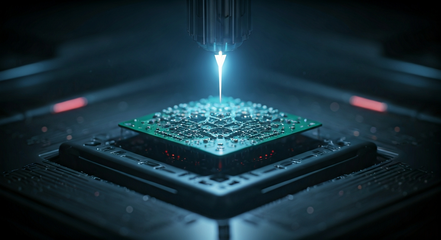
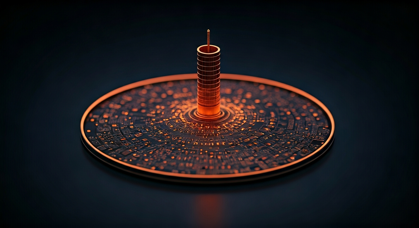
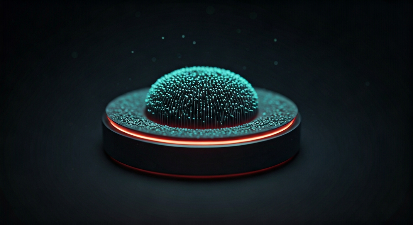
json { "headline": "Post-2030 Nanomanufactured Plasmonic Terahertz Nano-Antennas", "summary": "This document outlines the advanced nanotechnological additive manufacturing (3D printing) approach for producing plasmonic nano-antennas optimized for Terahertz (THz) frequencies. Leveraging post-2030 capabilities, it integrates novel nanomaterial feedstocks, advanced laser-based processes, precise piezoelectric actuation, and AI-driven autonomous production lines to achieve unprecedented performance and on-demand fabrication.", "body": "## Target Device & Specifications\n\nThe target device is a plasmonic nano-antenna designed for efficient operation in the Terahertz (THz) spectrum (0.1-10 THz). Key specifications include sub-wavelength resonant structures with feature sizes in the tens to hundreds of nanometers, high directivity, broad bandwidth, and low Ohmic losses. The antenna will be designed for integration into compact THz sensing, imaging, and communication modules. Material properties will be precisely tuned to maximize surface plasmon resonance (SPR) enhancement at target THz frequencies.\n\n## Nanomaterial Feedstocks\n\nFeedstocks will consist of precisely engineered nanocomposite inks and powders. These include: 1) Plasmonic nanoparticles (e.g., gold, silver, aluminum, or novel alloy nanoparticles) functionalized for self-assembly and dispersion. 2) Dielectric nanomaterials (e.g., high-k dielectrics, functionalized polymers) for precise control of electromagnetic environment and structural support. 3) Conductive nanomaterials (e.g., carbon nanotubes, graphene flakes, metallic nanowires) for enhanced conductivity and integration with electronic components. These materials will be supplied in stable colloidal suspensions or fine, uniform powders with controlled particle size distribution and surface chemistry, compatible with advanced additive processes.\n\n## Nanoscale Additive & Laser Process\n\nThe primary additive process will be a hybrid Femtosecond-Laser Direct Writing (FLDW) and advanced Two-Photon Polymerization (TPP) system. FLDW will be used for direct deposition and structuring of metallic nanoparticle inks, enabling atom-by-atom or cluster-by-cluster assembly of plasmonic elements with sub-nanometer precision. TPP will be employed for fabricating intricate dielectric scaffolds and antenna geometries, achieving resolutions below 50 nm. Laser-Induced Forward Transfer (LIFT) will be utilized for precise deposition of thin films and functional layers. Nanoscale Selective Laser Sintering (nSLS) of metallic nanopowders will be an alternative for creating larger, yet still nano-featured, metallic antenna elements when extreme precision in TPP/FLDW is not required.\n\n## Piezoelectric & Nanopositioning Integration\n\nThe additive manufacturing platform will be built upon ultra-high precision, multi-axis piezoelectric stages capable of sub-nanometer resolution and stability. These stages will provide the foundation for the laser optics and the build platform, ensuring accurate positioning of the laser focus and the workpiece during fabrication. Active feedback mechanisms, potentially incorporating in-situ interferometric metrology, will be used to compensate for thermal drift and mechanical vibrations, maintaining positional accuracy at the nanoscale throughout the entire printing process. This ensures the geometric fidelity required for optimal THz plasmonic behavior.\n\n## Autonomous Production Line\n\nThe production line will be fully autonomous, driven by AI and machine learning algorithms. An AI design engine will optimize nano-antenna geometries based on desired THz performance parameters and material constraints. The AI will then translate these designs into machine instructions for the additive manufacturing hardware. Self-directed calibration and error correction routines, utilizing in-situ metrology and predictive maintenance, will ensure continuous operation. Self-assembly principles will be integrated into the material feedstocks and fabrication steps, guiding the assembly of nanoscale components into the final antenna structure with minimal external intervention.\n\n## Key Challenges & Yield\n\nKey challenges include achieving defect-free nanoscale structures, controlling material interfaces and their electronic properties, managing thermal effects during laser processing, and ensuring reproducibility across different fabrication runs. Achieving high yield for nanoscale devices is inherently difficult. The autonomous system will focus on real-time defect detection and correction, adaptive fabrication strategies, and process optimization to maximize yield. Initial yields may be low, but continuous AI-driven learning is expected to rapidly improve this metric. The ability to "print and test" within the same automated cell will be crucial for rapid iteration and improvement.\n\n## Test & Qualification\n\nIn-situ metrology will be integrated throughout the fabrication process. This includes atomic force microscopy (AFM) for surface topography, optical microscopy for feature verification, and potentially THz near-field scanning optical microscopy (SNOM) for immediate functional assessment of plasmonic behavior. Post-fabrication, full THz spectroscopy, impedance matching measurements, and radiation pattern analysis will be performed. Automated quality control loops will use these results to refine future fabrication parameters, enabling a closed-loop optimization system.\n\n## TRL & Post-2030 Roadmap\n\nThis technology is envisioned to be at TRL 6-7 by 2030, with significant advancements in AI control and nanomaterial stability. The roadmap includes: 1) 2025-2027: Development of stable, high-concentration plasmonic nanocomposite inks and advanced piezoelectric stages. 2) 2027-2029: Integration of AI-driven design and fabrication control, achieving proof-of-concept antenna prototypes. 3) 2030 onwards: Full autonomous production line demonstration, scaling up to batch production and integration into application-specific modules. Further development will focus on multi-material printing and in-situ repair capabilities.\n\n## Applications (incl. in-situ fabrication in space/Mars)\n\nApplications span high-bandwidth THz communication, ultra-sensitive chemical and biological sensing, advanced medical diagnostics, and security screening. The autonomous, on-demand nature of this manufacturing process is ideal for in-situ fabrication in resource-constrained environments like space stations or Martian colonies. Manufacturing THz components directly on-site reduces launch mass and lead times, enabling rapid deployment of critical infrastructure for exploration, research, and settlement. This capability is fundamental for achieving self-sufficiency in off-world habitats."

}
json { "analysis": "On-demand nanomanufacturing of plasmonic THz antennas via advanced additive processes is critical for a self-sufficient multi-planetary civilization. It enables the localized production of highly specialized components, reducing reliance on Earth-based supply chains. This drastically lowers mission costs and increases operational flexibility. The ability to fabricate complex nanostructures in situ on Mars or space stations for communication, sensing, and scientific instrumentation is a cornerstone of sustainable off-world presence and exploration." }
Cross-Model Verification (GPT-3.5)
- The use of sub-nanometer precision in the assembly of plasmonic elements via Femtosecond-Laser Direct Writing is physically implausible due to diffraction limits. - Achieving defect-free nanoscale structures and high yields in nanoscale device production is challenging and may be overstated, especially with reference to "self-assembly principles." - The claim of autonomous in-situ fabrication in space or Mars lacks detail and feasibility assessment, particularly in terms of resource availability and environmental conditions. - The integration of AI for optimizing nano-antenna geometries based on material constraints and THz performance parameters is a plausible advancement. - The incorporation of in-situ metrology like AFM and optical microscopy for quality control during fabrication is a credible approach. - The roadmap for technology development and the application areas of plasmonic nano-antennas in THz communication and medical diagnostics are realistic and well-aligned with future trends.
This content was produced by the news editor with AI.