Autonomous Nanoscale Additive Manufacturing of High-Performance Waveguide Antenna Feeds
This post-2030 technology envisions a fully autonomous, AI-driven production line capable of manufacturing complex waveguide antenna feeds with sub-nanometer precision using advanced nanomaterial feedstocks and laser-based additive processes. Integrated with sophisticated piezoelectric actuation and nanopositioning systems, this system will enable on-demand, in-situ fabrication of highly efficient RF components, revolutionizing space and planetary exploration.
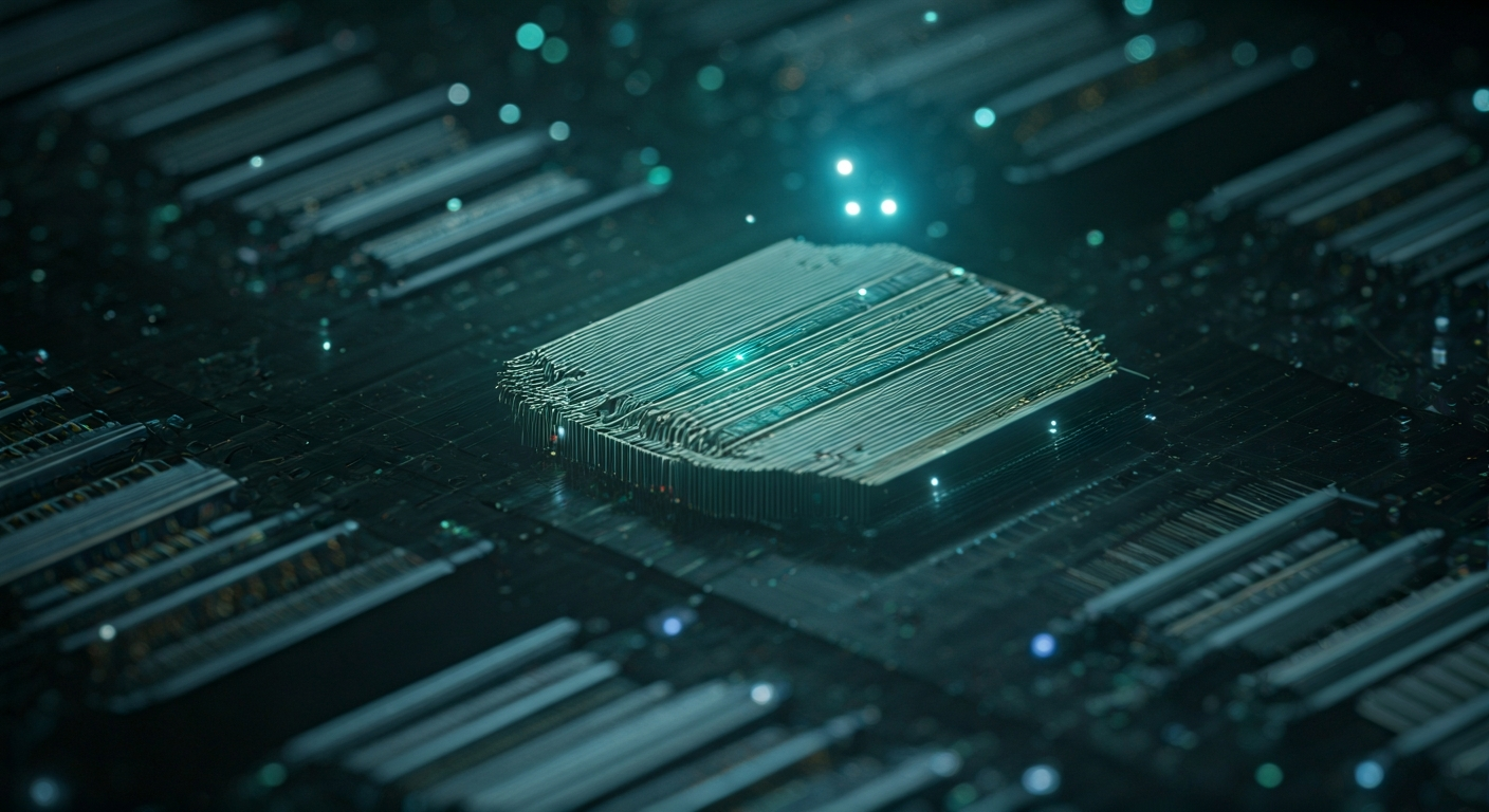
Target Device & Specifications The target device is a high-performance waveguide antenna feed, designed for precise electromagnetic wave manipulation. Key specifications include:
* **Frequency Range:** 30 GHz to 1 THz (covering millimeter-wave and sub-terahertz bands). * **Dimensional Tolerance:** Sub-wavelength precision for critical features (e.g., waveguide dimensions, transitions, apertures) to minimize signal loss and maximize efficiency. Aiming for < 1 nm surface roughness. * **Material Purity:** Ultra-high purity nanomaterials to ensure predictable electromagnetic properties and minimize dielectric/conductive losses. * **Complexity:** Ability to fabricate intricate internal geometries, including multi-mode structures, polarization converters, and integrated filters, with complex external interfaces for direct integration with radiating elements. * **Robustness:** Material properties and structural integrity suitable for demanding environments (vacuum, radiation, thermal cycling).
Nanomaterial Feedstocks The manufacturing process will utilize a range of advanced nanomaterial feedstocks, delivered via controlled aerosol or ink-jet systems:
* **Conductive Nanomaterials:** Graphene nanoplatelets, carbon nanotubes (CNTs) with controlled chirality, metallic nanoparticles (Au, Ag, Cu) stabilized in a low-viscosity, photo-curable matrix. These will form the conductive walls of the waveguide. * **Dielectric Nanomaterials:** Precisely engineered ceramic nanoparticles (e.g., SiO2, Al2O3, TiO2) or advanced polymers with tailored dielectric constants and low loss tangents, used for dielectric loading or as sacrificial/support materials. Nanoparticle-based composites will offer tunable properties. * **Quantum Dot (QD) Infused Polymers:** For potential active elements or enhanced optical/RF coupling, QDs with specific emission/absorption spectra can be incorporated. * **Self-Assembling Nanoparticles:** Pre-functionalized nanoparticles designed to self-assemble into specific crystalline or ordered structures under external stimuli (e.g., electric fields, light), enabling rapid formation of complex lattice structures or precise deposition.
Nanoscale Additive & Laser Process A hybrid laser-based additive manufacturing approach will be employed:
* **Two-Photon/Multiphoton Lithography (TPL/MPL):** For fabricating highly intricate, sub-wavelength dielectric structures and molds with resolutions down to tens of nanometers. This process will be used for creating the waveguide channels, dielectric lenses, or precise internal features. * **Femtosecond Laser-Induced Forward Transfer (fs-LIFT):** Ideal for direct, high-resolution deposition of metallic or conductive nanoparticle inks onto substrates. The ultrashort laser pulses enable precise transfer with minimal thermal damage, creating conductive traces and waveguide walls with high fidelity. * **Nanoscale Selective Laser Sintering/Melting (nSLS/M):** For building up conductive or dielectric structures from nanoparticle powders or pre-compounded feedstock. This will be used for creating larger waveguide sections or structural supports, potentially using focused Bessel beams for extended depth of focus and reduced scattering. * **Laser-Induced Plasmonic Assembly:** Utilizing localized surface plasmon resonance (LSPR) to guide and assemble metallic nanoparticles into desired conductive pathways or structures, enhancing conductivity and reducing losses.
Piezoelectric & Nanopositioning Integration Achieving the required precision necessitates advanced actuation and positioning:
* **Piezoelectric Actuators:** High-bandwidth, multi-axis piezoelectric stages will provide ultra-fine, sub-nanometer positioning of the laser focal spot, the substrate, or the material feedstock delivery nozzle. These will be integrated into a vibration-isolated platform. * **Closed-Loop Feedback Systems:** Real-time monitoring using atomic force microscopy (AFM) or scanning electron microscopy (SEM) integrated into the build chamber will provide feedback for precise path control and error correction, ensuring dimensional accuracy and surface finish. * **Active Vibration Damping:** Advanced active damping systems will counteract environmental vibrations, crucial for maintaining sub-nanometer stability during the additive process. * **Nanoparticle Manipulation:** Electric or magnetic field gradients generated by integrated micro/nano-electrodes will be used in conjunction with piezoelectric stages to precisely guide and deposit self-assembling nanoparticle clusters.
Autonomous Production Line The entire manufacturing process will be managed by an AI-driven control system:
* **AI-Powered Design Optimization:** Generative design algorithms will optimize waveguide feed geometries for specific performance requirements, material properties, and manufacturability constraints. * **Self-Directed Process Planning:** The AI will translate the optimized design into a sequence of additive steps, selecting appropriate laser parameters, material feed rates, and positioning trajectories. * **In-Situ Monitoring & Adaptive Control:** AI will analyze real-time sensor data (optical, acoustic, thermal, dimensional) to detect defects, deviations, or material inconsistencies and autonomously adjust process parameters to correct them. * **Self-Calibration & Repair:** The system will perform automated self-calibration of its positioning and laser systems. For minor defects, localized laser-based repair or material re-deposition will be initiated. * **Self-Assembling Workflows:** Leveraging the inherent properties of programmed nanoparticles, the AI will orchestrate external stimuli to guide self-assembly processes, reducing reliance on purely subtractive or additive deposition.
Key Challenges & Yield
* **Material Homogeneity & Control:** Ensuring uniform dispersion and controlled aggregation of nanoparticles in feedstocks is critical. Inconsistent feedstock can lead to variable conductivity and dielectric properties. * **Surface Finish & Electromagnetic Performance:** Achieving sub-nanometer surface roughness within complex internal geometries is paramount for minimizing RF losses. Achieving this with additive processes, especially for THz frequencies, is a significant hurdle. * **Defect Detection & Mitigation:** Identifying and correcting nanoscale defects (voids, agglomerations, misalignments) in real-time is challenging. Yield will be heavily dependent on the efficacy of in-situ monitoring and adaptive control. * **Scalability & Throughput:** While precision is key, achieving reasonable production throughput for complex waveguide feeds will require optimization of laser powers, scanning speeds, and parallel processing capabilities. * **Environmental Control:** Maintaining an ultra-clean, controlled atmosphere within the build chamber is essential to prevent contamination and ensure material integrity.
**Expected Yield:** Initial yields for highly complex, sub-wavelength structures might be in the 30-50% range, improving to 80-90% with mature AI control and advanced material feedstocks. Simpler waveguide sections could achieve higher yields.
Test & Qualification
* **In-situ Metrology:** Integrated AFM/SEM for dimensional verification and surface analysis during or immediately after fabrication. * **Non-Destructive Testing (NDT):** High-resolution X-ray computed tomography (CT) for internal defect detection. Terahertz time-domain spectroscopy (THz-TDS) for material property characterization and loss assessment. * **RF Performance Testing:** Vector Network Analyzers (VNAs) capable of operating at target frequencies (up to 1 THz) to measure S-parameters, insertion loss, return loss, and radiation patterns. * **Environmental Stress Testing:** Accelerated aging tests simulating vacuum, thermal cycling, and radiation exposure.
TRL & Post-2030 Roadmap
* **Current TRL (2024):** TPL/MPL (~TRL 6-7 for micro-scale), fs-LIFT (~TRL 5-6), nSLS (~TRL 7-8 for macro-scale). Nanomaterial feedstocks for precise RF applications are emerging. * **Post-2030 Roadmap:** * **2030-2032:** Integration of advanced nanomaterial inks with fs-LIFT and TPL for multi-material printing of basic waveguide components. Development of initial AI process control modules for defect detection and compensation. TRL 6-7. * **2033-2035:** Realization of fully autonomous, closed-loop manufacturing for standard waveguide feed designs. Integration of self-assembly techniques for conductive pathways. Achieving < 5 nm surface roughness. TRL 8. * **2036-2039:** Expansion to complex, multi-functional waveguide antenna feeds (e.g., reconfigurable, integrated filtering). Demonstrating on-demand, in-situ fabrication capabilities. Achieving sub-nanometer surface finish and >95% yield for optimized designs. TRL 9.
Applications (incl. in-situ fabrication in space/Mars)
* **Satellite Communication:** High-frequency, lightweight, and compact waveguide feeds for next-generation satellite constellations, enabling higher data rates and improved bandwidth. * **Deep Space Probes:** On-demand fabrication of custom RF components for missions where mass and volume are critical, and replacement parts are impossible to transport. This includes manufacturing directly on the probe. * **Lunar/Martian Bases:** In-situ resource utilization (ISRU) for fabricating essential communication and sensing equipment. Local regolith could be processed into nanomaterial precursors for printing. * **Advanced Radar Systems:** Highly precise waveguide feeds for high-resolution radar systems used in planetary surveying, autonomous navigation, and environmental monitoring. * **Quantum Computing Interconnects:** Precision waveguide structures for coupling microwave or THz signals to superconducting qubits or other quantum devices. * **Terahertz Imaging & Spectroscopy:** Fabrication of complex THz optical components for scientific instruments and advanced imaging systems on extraterrestrial platforms.
Analysis On-demand nanomanufacturing of waveguide antenna feeds is a cornerstone for a self-sufficient multi-planetary civilization. It enables the rapid, localized production of critical communication and sensing infrastructure, reducing reliance on Earth-based supply chains. By allowing components to be fabricated from local resources (ISRU) or on-demand in space, it drastically cuts launch costs and lead times. This capability is essential for establishing robust communication networks on Mars, the Moon, and beyond, facilitating scientific research, resource management, and long-term human presence.
Cross-Model Verification (GPT-3.5)
- The frequency range of 30 GHz to 1 THz for the waveguide antenna feed is technically feasible, but the dossier lacks specific details on how the design accommodates such a broad bandwidth effectively. - The claim of aiming for < 1 nm surface roughness for critical features is ambitious and may be challenging to achieve consistently across complex geometries using current additive manufacturing techniques. - The integration of Quantum Dot (QD) infused polymers for enhanced optical/RF coupling is a novel concept but lacks specific data on the performance improvement or practical implementation. - The mention of utilizing focused Bessel beams for reduced scattering in Nanoscale Selective Laser Sintering/Melting (nSLS/M) is a cutting-edge approach, but the effectiveness and feasibility need more detailed elaboration. - The autonomous control system for managing the manufacturing process is plausible, but the dossier could benefit from more information on real-world testing/validation of the AI-driven system in similar additive manufacturing scenarios.
This content was produced by the news editor with AI.